
Physical Cell ID Planning
PCI planning is one of the most important things to understand while planning an LTE network and it is usually left untouched in most of the LTE manuals and text-books. As already explained, the PCI is decoded using the SSS and the PSS and can be given by the following equation
PCI = 3*SSS + PSS
Where, PSS = 0,1,2
SSS = 0,1,2, . . . . 167
PCI = 0,1,2, . . . . 503
So, if SSS is equal to 5 and PSS is equal to 1 then the PCI would be 16. A basic rule of thumb is that the neighboring cells should not have the same “PSS” value. Usually, a site with 3 cells use same SSS value but different PSS value such that the PCIs for cell 1,2 and 3 will be 0,1 and 2.
Within the cell, the channels are scrambled using the PCI which means that the PCI serves as the seed for the cell’s permutation algorithm. That’s why, the UE has to decode the PSS and SSS before reading any other channel as it needs to get the PCI which tells about the permutation used in the cell.
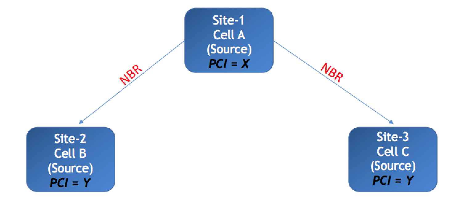
Rule#1 Usage of same PCI
Since we have 504 PCIs so this rule is usually not difficult to follow.
- The same site should not use the same PCI again on the same frequency
- The NBRs of the site should not have the same PCI on the same frequency
- Ideally, two NBRs of the site should not have same PCI between them. For instance, Cell-A has NBR Cell-B and Cell-C and both of them have the same frequency, then the PCI of Cell-B and Cell-C should not be identical. This is difficult to maintain in a LTE network but this issue can cause PCI confusion and handover failures
Rule#2 PCI mod3 & mod6
Let’s dig a bit deeper and understand how different vendors do the PCI planning. One approach is to use the same group (same SSS) on one site (3 sector sites) which is the PCI-Modulus3 planning technique. This is much similar to what is depicted in the Figure 9 (above). The PCI is also used to indicate the location of RS along the frequency axis. Consider that the PCI=X will have the RS located at the first sub-carrier then the PCI=X+1 will move the RS downwards by one sub-carrier and PCI=X+2 will move it down by another sub-carrier. The point to note is that there are 2 RS per RB per antenna port in the 1st OFDM symbol. But there are another 2 RS for the second antenna port on the same symbol. These 2 RS are zero-powered (also known as DTX – discontinuous transmission) on the first antenna port. So, when the PCI is changed to X+3, then the RS for antenna port0 moves to the same position as RS for antenna port1 of the PCI=X. This means that for every PCI=X, any other PCI with value of X+3(n) – where “n” is an integer, will have a collision on Reference Signal between the two ports. This is known as the PCI mod3 issue.
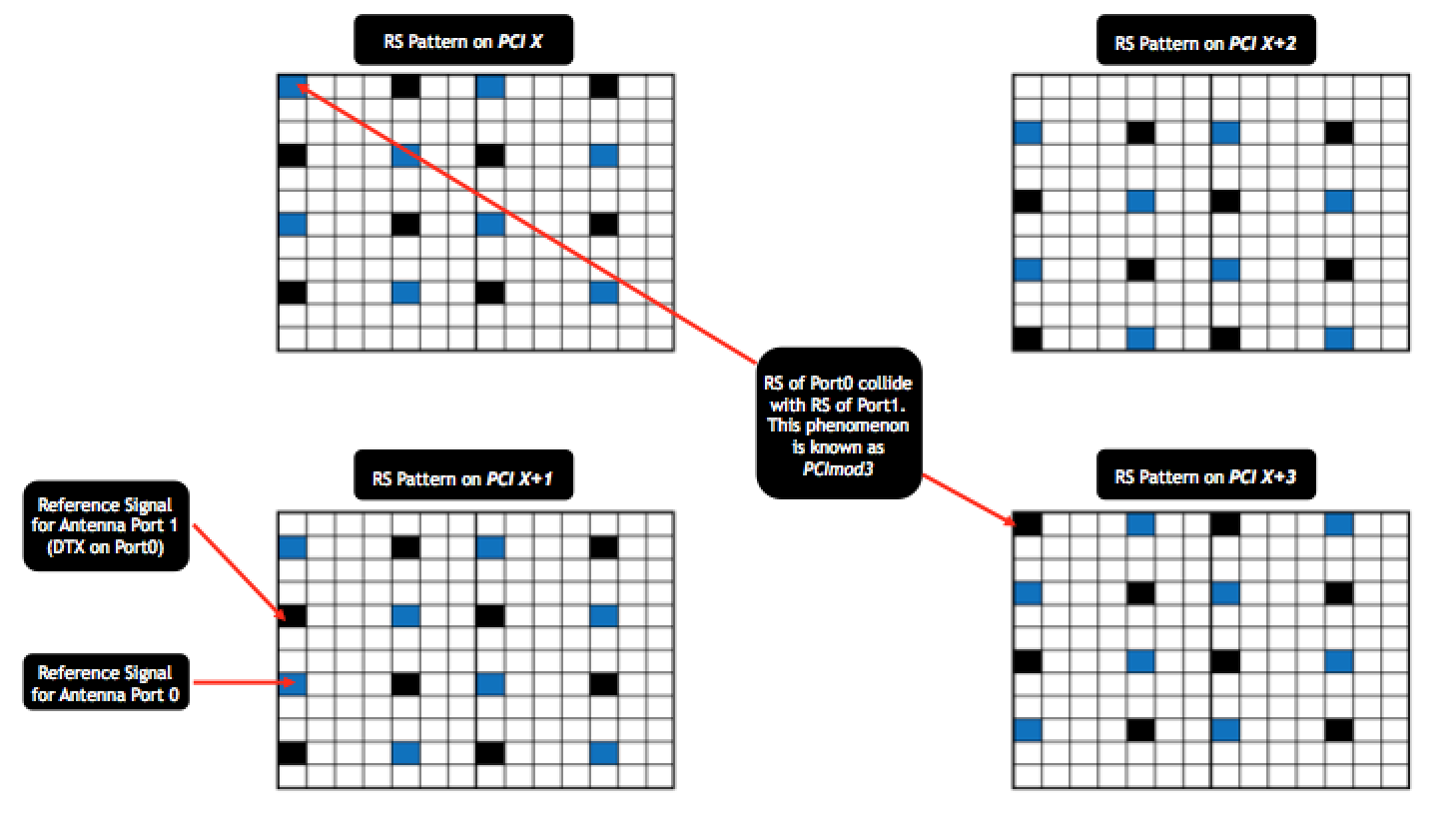
However, if the system is only a single port system like most of the IBS systems, then the PCI mod3 will not impact because there will be no reference signals on the second port. Instead, the rule will change to PCI mod6.
An important point to remember is that most of the FDD LTE networks are not time synchronized between sites so the symbols do not usually overlap in time. Therefore, for FDD systems, this rule is not as important as it is for TDD LTE systems which are always time synchronized.
Rule#3 PCI mod30
Just like in downlink, every 3rd or 6th PCI collides on the reference signals, every 30th PCI has the same pattern of uplink reference signals. In uplink, the reference signals are present in the central symbol of the slot and their pattern or base sequence repeats for every 30th PCI. In case, two adjacent cells have same PCI mod30, then the cell can have difficulty in decoding which can result in higher block error rate in uplink. However, this is not a critical issue and very rarely observed in the commercial networks.
Rule#4 PCFICH collisions
In LTE, the PCFICH is one of the channels that gets its location determined based on the PCI. This also means that every PCFICH will repeat its position for some PCIs. Basic rule is that every 50th PCI will have same location of PCFICH for 20MHz channel while every 25th PCI will have same location of PCFICH for 10MHz channels. Such a scenario can cause decoding failures or higher block error rate on PCFICH and since PCFICH is required to decode PDCCH so it can cause DTX (decoding failure of grants on PDCCH).
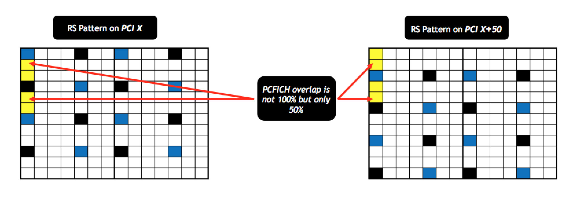
But once again it is difficult to observe in FDD systems and another fact that most of the documents overlook is that PCFICH consists of 4REGs. Each REG has 4 REs but we have reference signals in a LTE system after every 2 REs. So, each PCFICH REG will have Reference Signals embedded inside and that means that 2 PCFICHs usually do not overlap each other completely.
Rule#5 SSS Correlation Issue
There is another known rule that is not really considered as it has no evident impact but I thought it is worth mentioning. As explained, each PCI is made up of PSS and SSS. Each SSS is made up of two length-31 binary m-sequences (m0 and m1) but since SSS are 168 in count so these length-31 sequences are bound to repeat. So, each time m0 or m1 repeat itself, the overall correlation between those 2 SSS values is much higher – in other words such SSS can interfere with each other. As an example, SSS value of 9 can have interference with 10 other SSS values.
However, this type of interference has no effect on KPIs and if the UE fails to decode SSS in first subframe, it can still decode it in the 6th subframe as SSS repeats twice within 10ms. So, such an issue, if observed might delay network entry by 5 to 10 ms which does not have any considerable impact.
If you have any questions or feedback regarding PCI Planning, simply drop a comment below and I will surely get back to you. Also, If you liked this article, then please subscribe to our Youtube channel – Our Technology Planet for more exciting stuff and videos.
Ali Khalid
Latest posts by Ali Khalid (see all)
- 5G Coverage Expansion Analysis – Find The Optimal 5G Coverage Threshold For Your Network - November 9, 2024
- 5G Coverage Expansion - November 9, 2024
- 5G SA Cell Search & Network Entry Matrix - July 18, 2023
That is nice article from you , this is informative stuff . Hope more articles from you . I also want to share some information about Best Digital marketing service in india
Dear Ali Khalid,
thanks for your article.
Can you please, explain us the PCI planning rules for nb-IoT?
Regards,
Ivan
Hello Ivan,
Thank you for your comment.
Please follow the link below and post your question/feedback in Youtube comments section so that Ali Khalid will be able to answer.
PCI Planning – https://youtu.be/x4OKyi6O3FY
Hi Khalid
What is the impact of having different PCIs on the same sector??
Hi,
for Rule#3 PCI mod30, does it mean that for every X, these are some of the examples which are allowed to be NBR:
– X+1,
– X+2,
– X+4,
– X+5,
– X+7,
– X+8 etc
Thanks in advance!
Yeah, your understanding is correct
Does this change for a TDD system? Is using Mod3 the best PCI allocation for a TDD system?
Which is not quite possible right? Haha
What are your suggestions for PCI planning in 6 sector network?
We are planning network expansion of some 200 sites from 3 to 6 sector for capacity issues, but need to prepare the best PCI plan
You cannot really do much with 6 sector sites so just try to ensure that adjacent cells are not PCI mod3
is there any problem if i assign same mod which is in my neighbor cell ?
If the cells are time synced then same mode will have RS interference.
Thanks Khalid, i really enjoyed reading, as it looks soo simple to understand.Please keep posting.
Thanks Suresh 🙂
What will be the impact when cell specific reference signal collides due to mod-3 conflict? Will there be an issue in measuring the power?
Mod-3 conflict will cause RS collision, reducing RS-SINR. No, the power by itself is not impacted.
What would be the impact when there is a collision in the cell specific reference signal?
It will impact RS-SINR and can reduce throughput and impact decoding at the UE end.
Sir
How can we plan PCI for 4th sector addition in same Band
salam Ali khali ,
what do you think about 6 sector LTE deployement for rural Area ( Isolated area )
BR
Hi,
do you know why some UE type(certain FGI) has a HO problem towards cell with PCI 0? Measurement reports show RSRP=-43 all the time from same FGI and when instructed to HO it fails.
Interesting case. I haven’t heard about it so do let me know if you happen to root-cause it.
Hi Ali Khalid,
NIce article. In cell edge it is common that UE see more than 3 cells, so that means PCI mod 3 issue is unavoidable there ?
Yeah, at such scenarios where multiple cells overlap, then yeah it is pretty much unavoidable.
Can you pls explain on DMRS base sequence by relating it with PCI and mod 30
Hi,
Why I cant use Mod6 with Two TX Antennas?
Is this because more RE’s will be unused on other Antenna Port?
For 2 antennas, every 3rd PCI’s RS will overlap and every 6th PCI’s RS will also overlap. So, mod6 rule only applies to single antenna system.
Great Article, Many thanks
Rule#4 PCFICH collisions
“PCFICH is mapped to 4 REGs (labeled p, q, r and s in Figure 2) which are equidistant and spread across the bandwidth in frequency domain. These four REG locations are a function of PCI and the deployed bandwidth. In time domain, it is mapped to the first OFDMA symbol of the subframe (see Figure 1). LTE defines a REG (Resource Element Group) as 4 useful REs (Resource elements) or modulation symbols grouped together. But with 2 MIMO Reference signals associated, 6 REs are grouped into a REG in the first OFDMA symbol of the subframe (Figure 2 shows sample position of Reference signals marked as x).”
Source : http://lteuniversity.com/get_trained/expert_opinion1/b/manohara/archive/2013/05/01/don-39-t-forget-pcfich-while-doing-physical-cell-identity-pci-planning.aspx
Formula in the bottom for PCFICH segment calculation => http://www.sharetechnote.com/html/Handbook_LTE_PCFICH.html
Can you clarify (if you can kindly refer to link 2) the calculation as evident from link 1 specially in case of 5 MHz example , there are weird values of PCFICH REGs (p=72 , q=144 , r=222 . s=294 for PCI 12)
And also the formula used (link 2) provides what output and what is NRB_SC in the formula and i assuming NCell ID refers to PCI
http://niviuk.free.fr/lte_resource_grid.htm
http://www.simpletechpost.com/2013/09/physical-control-format-indicator.html
Ok , i understood NRB_SC is number of sub carriers within a RB
And formula provides the Sub Carrier index within the BW
Hi Ali,
I am constantly amazed by your ingenuity while exploring and explaining the LTE stuffs. One more request could you please add something to paging related planning. How much paging can a eNB is capable of handling from MME . When it can discard and all.
Regards
Prakash
Thanks for the kind words, Prakash. Sure, I will put that in my list of topics 🙂
VERY nice article, keep up the good work!
Thanks
Excellent article. How can I solve the mod 3 issue when I must use five beam antennas? I mean, I will have RS interference among neighbours sites? Taking into account that the five sectors will have at least one neighbor from nearby sites. in this particular scenario, is the interference unavoidable?
Yeah that is an issue with the mod-3 that it cannot be totally eliminated in any network and especially if you have more than 3 sectors. However, as I explained above, if it is an FDD system, the impact is usually lesser compared to TDD. But within the same eNB, the clock sync is usually same so the sectors are time synchronized. In this case, you should verify that adjacent sectors do not have same mod-3.
Hi, Can you please explain further how to improve SINR for 6 sector TD-LTE sites planned with Mod-3 PCI Plan .
Thanks in advance .
Well the answer is similar. Since we have overlap of RS for every mod3 PCI, so there always has to be a compromise with more than 3 sectors. You may use same PCImod3 value in sectors without coverage overlap or looking in opposite direction. Do bear in mind that you should ensure backlobe suppression in this case.
Thanks lot !! Very well-defined .
Is there any possibility of parameter tuning to improve SINR in this scenerio ?
Great article , for sites that have 4 sectors or more , you can make SFN solution in Huawei , it is combine two physical cells into one logical cells , so if you have 4 physical cells , they will be 3 sectors , so you will not have the same PCI in the same eNodeB.
The drawbacks of this solution is it will impact the capacity as it make on cell serve in area that need 2 cells.
Also it will make wider interference in cell edge users.
Yeah that is a good idea. ASFN might help in that case to further reduce the drawbacks.
Yeah , I agree with you, I tried ASFN , and with tunung it’s Paramters , cell utilization was deceased , but ASFN needs the SRS to be ( default ) configuration not Adpative.
Hi Juan!
usually in this case, vendors provide solution to group 2 sectors (beams) into a single cell in other to keep not more than 3 logical cells (currently up to 6 sectors can be grouped into 3 cells) and still benefit from PCImod3 benefits. Huawei for example suggest 4T4R as an option for the same purpose…
Thanks for the information!
Could you please tackle as well the PCI planning strategy when various CA (intra/inter-band) multiple CCs are activated?
Can you elaborate your question please? Multiple CCs serve as interfrequency NBRs and usually interfrequency co-sector NBRs have the same PCI e.g. if L800 has PCI 3 then its co-sector L1800 usually also has PCI set to 3 and they will work as PCC and SCC with the same PCI. If I am missing something, feel free to add 🙂
Great article. I’ve been cleaning up various PCI mis-alignments in my network. One additional rule is to maintain the same PCI across Inter-freq carriers of the same sector face. I’ve found that there can be an observer improvement in Inter-freq handover and drop call rates.
Thanks why is that so…?
This is an interesting observation that you have made. Can you elaborate as I have not seen definite proof of this yet.
I think this is a normal rule, as we put same PCI for each sector with differents Band.
so F1 and F2 of sector 1 have the same PCI of course.
what’s the original in this rule ? is there any one who don’t make this rule ? because it’s easier way to decrease the complexity of palnning (reduce the work by 2).
BR
Agreed, that is the most convenient way to do the planning.
Hi Kamel,
Though the frequencies are different, still the placement of RS is same as it is based on only PCI and not on the frequency. How this method avoids PCI mod 3 problem ?
Its different frequency !
Very good explanation with practical impact on network planning.
Rule#3 PCI mod30 , -Could you please explain about uplink RS ? For every length at least 30 sequences should be available (for bandwith bigger than 72 subcarriers more sequences could be available) for DRS , is it correct reason for PCI mod30 collision concept ?
UL DMRS are based on sequence-group number which is defined by a group hopping pattern and a sequence-shift pattern. Simply put, the shift pattern within itself is determined with a mod30 equation based on the PCI. So, for all bandwidths, the UL DMRS pattern will repeat for every 30th PCI. The impact is not usually observed as it is difficult to have a perfect overlap in FDD systems between two different eNBs and then considering the relatively low load in uplink , it is difficult to get an overlap between users (who are on different cells) on the same time and frequency resources
Dear
In Nokia, we define UL DMRS as below:
U = (PCI + grpassignPUSCHGroup)mod30 should be respected in the planning.
In case i have PCImod3 or 6 respected, i put grpassignPUSCH group to 0 else i put a value from 0 to 29.
My question is (1) how to define the sequence-shift pattern ? (as you said UL DMRS are based on sequence-group number which is defined by a group hopping pattern and a sequence-shift pattern).
(2) as i understand this U is used only for PUSCH DeModulation (DM), what about PUCCH DM RS ?
Thanks in advance.
In simple words, for PUSCH, the sequence shift is defined with PCI and a delta sequence which ranges from 0 to 29. So, if you change this grpAssign parameter you can change the U. For instance, you have two cells with PCI 30 and 60 so they have mod30 conflict. If you change the value of grpAssign for one of them to 1 then that should resolve their confict.
For PUCCH, the sequence is only PCImod30 and there is no delta sequence. So, in above case, you might be able to avoid conflict on PUSCH but not on PUCCH.
Can you please write us for PMI,RI,CQI
I will add this in my list. Stay tuned 🙂
Rule#3,4,5…Good addition which is not explained by most of writers…. i hope to expect more articles …
Thank you, Ashraf. I am glad you like it and I hope to write more soon.
Also request you to write about celledge throughout capacity planning.
Thanks Ali Khalid it very usefull to me. Could you plz elevorate little bit more about MOD6?
In simple words, Mod-6 is used in SISO systems (one Tx systems)
Maximum Perfection
Thanks, Abdullah.
Excellent
Thank you, Sufyan.
Need more guidelines in other LTE Topics. Kindly share mail ID to discuss.